Product
Menu
Solution
Menu
Technology
Menu
For Scientific Research & Industry Modernisation.
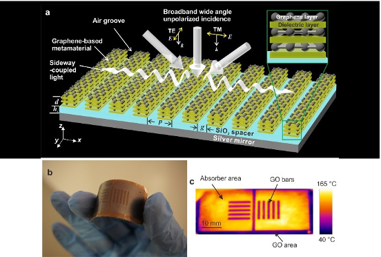
Graphene is the world’s thinnest yet hardest nanomaterial, with an extremely broad optical absorption covering the wavelength range of light from visible to microwave wavelengths. Its optical properties are non-dispersive, i.e., the absorption is the same 2.3% at any wavelengths. At the same time, it has a very high thermal conductivity (5300 W/m-K) and a resistivity of only about 10-6 Ω· cm, which is lower than copper or silver, and is currently the world’s smallest resistive material. Therefore, it is regarded as a key material for the future development of next generation electronic or optical components with thinner and better conductivity, and its applications include flat and ultra-thin lenses, transparent touch screens, optical panels, and even solar cells.
However, producing graphene films on a large scale is far from easy, requiring extremely complex processes and expensive vacuum equipment, and is limited to single-layer graphene on specific substrates (e.g., copper). When it is required to transfer graphene to other substrates (e.g., silicon) in applications, the transfer process is complex and requires multiple steps, while at the same time tends to destroy the structure of graphene and introduce defects.
On the other hand, in many applications (e.g. optical coating, rust prevention), the thickness of its single layer is not sufficient to provide the required effective optical modulation or effective protection. Therefore, stacking of multilayer graphene materials becomes necessary. However, simple stacking of graphene materials results in the formation of graphitic structures and thus loses the excellent properties of single-layer graphene.
Therefore, the challenge of how to increase the total thickness of graphene materials while maintaining the excellent properties of single-layer graphene becomes a conflicting need that has never been faced before.
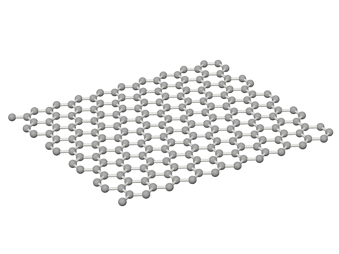
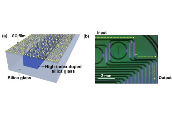
Based on the above needs, graphene metamaterials were created. Graphene metamaterials are designed (as shown in the figure) to maintain the excellent properties of a single layer of graphene by inserting a dielectric material between the single layers of graphene. Additionally, using this design, it is theoretically possible to infinitely stack graphene materials of any thickness to meet the requirements of the desired application.
As a kind of synthetic material, graphene metamaterials can not only maintain the excellent properties of single-layer graphene materials, but also realize extraordinary physical properties that conventional (or traditional) materials do not possess by adjusting their structural parameters, which can have far-reaching effects on new information technology, national defense industry, new energy technology, micro processing technology, etc.
Traditional methods of preparing graphene metamaterials require the manual stacking of single layers of graphene with dielectric materials by vapor phase deposition and transfer. The quality of the material depends entirely on the experience and ability of the operator and cannot be easily replicated. Also, the thickness and coverage area that can be achieved by this method are limited. The current world record thickness of graphene materials prepared using this method is 7 layers and the area is less than 100 microns. Thus the preparation and addition of multilayer graphene metamaterials remains a worldwide problem and challenge.
Innofocus has invented a revolutionary solution for the preparation of graphene metamaterials using a low-cost, no-transfer solution-phase method based on the principle of self-assembly. The method enables the growth of any number of layers of graphene metamaterials required on any substrate. The properties can also be tuned by selecting the nature and thickness of the dielectric material.
More importantly, this method enables the seamless wrapping and coating of micro-nano structures, thus maximizing their functionality (as shown in below figure).
Graphene metamaterials can be prepared on different substrates with arbitrary surfaces and shapes, such as silicon wafers, resin lenses, PET films, etc. (the thickness of the formed graphene metamaterials can be controlled to 3 nm in a single layer, and the flatness of the film is better than 10 nm)
The quality of the produced metamaterial is stable, does not vary with the number of layers, and the metamaterical can reach any layer with the thickness being precisely controlled.
Enables large scale coating up to 12 inches in diameter
Fully automated equipment which has low cost, good repeatability and saves labour
INNOFOCUS
Information can be encoded and stored and encrypted directly on graphene metamaterials using 3D laser nano-fabricating technology. It can also be applied to anti-counterfeiting.
The flat lens made based on the special synthesis principle of graphene metamaterial platform can work for a long time in microfluidic liquids for subwavelength focusing and imaging. The device optical focusing performance can be maintained in liquid environment for more than one month without significant degradation.
The ultra-high nonlinear optical properties of graphene metamaterials enable significant improvements in four-wave mixing efficiency, laying the foundation for highly integrated, flexible, and ultra-thin and ultra-light optical and photonic systems
Excellent solar spectral selectivity and omnidirectional absorption, as well as excellent photothermal performance and high thermal stability, enabling high-efficiency solar thermal conversion at large angles