

Product
Menu
Solution
Menu
Technology
Menu
For Scientific Research & Industry Modernisation.
The rapid advancement of information technologies in the 21st century has indicated the approaching post-Moore’s law era. Moore’s law, which dictates the doubling of transistors on microchips every two years, has driven traditional computing technology for many years. The demand for higher speed, larger bandwidth, lower energy consumption, and improved security and stability in information technologies continues to grow. However, as we near the physical limits of miniaturization, new approaches are needed to continue advancing computation.
Integrated Quantum Photonic Chips (i-QPC) have emerged as a promising successor to silicon chips. With the continuous development, i-QPCs which offer the desired features including high speed and low power consumption, has become the best solution for high-throughput communication technology. However, as i-QPCs move towards commercialization and industrialization, existing fabrication capabilities face significant challenges concerning precision, reproducibility, and scalability to fulfill the needs for R&D and manufacturing.
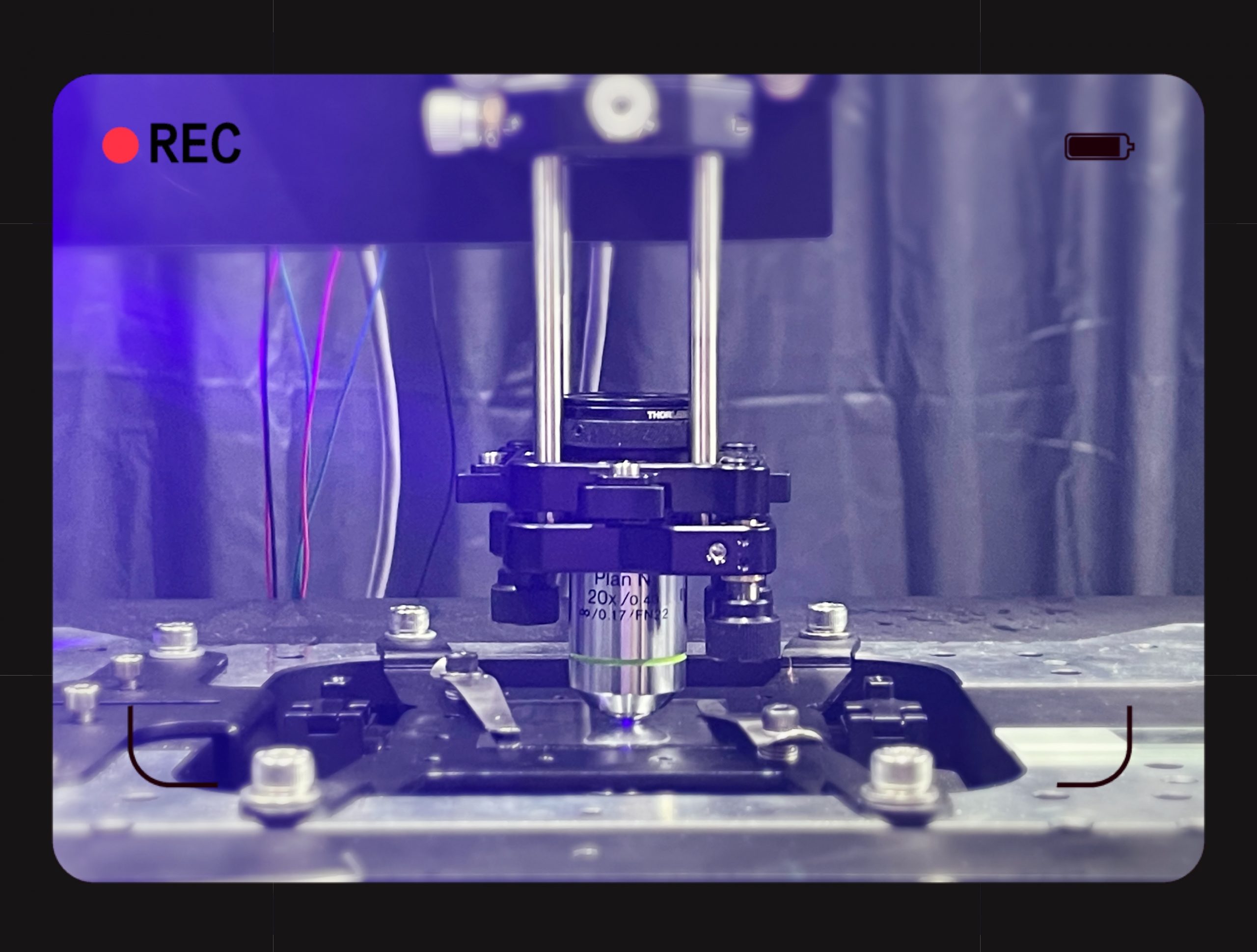
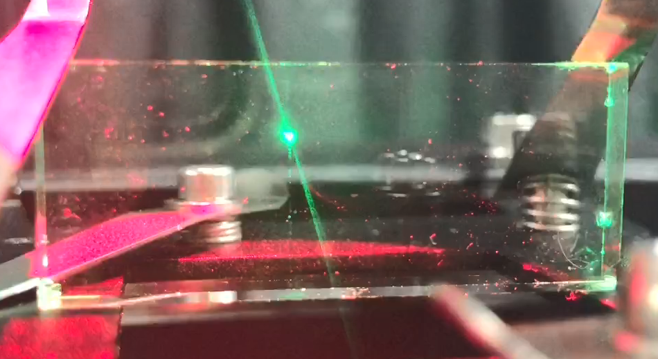
Conventional configuration of a laser nanofabrication system involves the segregation of distinct modules, with one dedicated to the fabrication process and another intended for characterization purposes. Therefore, users have to remove the fabricated sample in order to characterize it and then optimize the outcome, leading to a multi-stage and time-consuming process. This hence presents a challenge to the quality control of photonic chips and i-QPC. Additionally, the multi-stage process can introduce error, which results in insufficient correlations between the characterization results and the fabrication parameters.
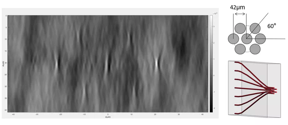
To efficiently and accurately characterize nanostructure/nanopatterns of 3D photonic chips has been long sought. However we are yet to find a method that can accurately characterize the refractive index distribution as well as the surface morphology of the optical materials. To fabricate 3D optical structures in optical crystals, the difference in refractive index introduced by laser processing is particularly important, which determines the design of the optical component and its loss.

To address these challenges, Innofocus developed the world-first intelligent laser nanofabrication system with our unique in-situ 3D refractive index imaging functionality i.e. HoloView 3DRI. The nanoLAB H3D model can achieve in-situ refractive index characterization to help users obtain quantitative data which indicates the variation of refractive index with the parameters changing. The nanoLAB H3D model allows on-line inspection of the fabrication outcomes and on-site correction of fabrication conditions, which totally revolutionizes the laser nanofabrication sector. It greatly reduces the time span required for the fabrication and characterization of photonic devices and chips like i-QPCs, meanwhile significantly increasing the laser fabrication accuracy and reproducibility. Users can apply these data to design and simulate the 3D optical waveguide structure to be fabricated, to achieve globally optimal result.
It represents the state-of-the-art and it is the world’s only commercially available high-resolution in-situ 3D refractive index distribution characterization equipment. Users can now perform characterization and optimize the fabrication results during the fabrication of sample, which greatly reduces the time cost involved. It enables users to obtain the optimum results in one shot. It provides unprecedented convenience for 3D optical waveguide and photonic chip processing. It provides more support for the industrial applications of laser nanofabrication such as optical communication, all-optical network and quantum optics. The equipment is expected to provide promising solution for the existing industry challenge faced by the development of i-QPCs.
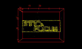
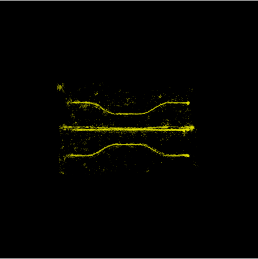
HoloView 3DRI, the 3D in-situ refractive index characterization system designed by Innofocus, has proved to enable characterize the 3D spatial refractive index distribution with our innovative optical imaging technology and image reconstruction algorithm. The system can precisely measure the refractive index distribution in material and effectively reconstruct the refractive index distribution, and form image of the 3D structure with an accuracy of 10-4. It is non-destructive and non-invasive, and it allows on-line inspection of the fabrication outcomes and on-site correction of fabrication conditions, making it valuable for the applications in the disciplines of 3D photonic chips, all-optical communications, sensors, biophotonic and micro/nano optical and photonic devices.
The key functions of the HoloView 3DRI system developed by Innofocus include:
along with the 3D spatial distribution of the refractive index and surface smoothness of femto-laser-processed optical components and structures. All of these can then contribute to optimizing laser processing parameters.

followed by a comparison with the original design input. This helps to ensure whether the fabrication outcome is optimal in terms of the desired quality requirements (e.g. self-inspection for defects and alignment with the design), allowing on-site correction of fabrication conditions of the optical components.
Therefore, the in-situ refractive index characterization system can be used to assess whether an optical component has been recharacterized. For example, in case of extreme conditions such as high temperatures or high humidity, it helps to examine if the component deform or sustain internal damage, and can identify which part of the component has suffered impairment.
While damage on the surface of components are easily detectable, internal damage caused by abrupt environmental temperature changes can hardly be found. However, such damage results in localized refractive index changes e.g. within the core of optical waveguide chips, or within FBGs, which can have detrimental impact on the performance of the optical components.
Currently, no other method can provide quantitative detection with high-resolution three-dimensional refractive index distribution measurements. This method stands as the sole approach for such detection in the industry.

HoloView 3DRI provides three-dimensional refractive index imaging display functionality which can visualize the observed refractive index distribution outcome. Based on the observed distribution, novel physical mechanisms of laser-material interactions can be discovered, displayed in a trustworthy and aesthetically pleasing manner through three-dimensional imaging.