
Product
Menu
Solution
Menu
Technology
Menu
For Scientific Research & Industry Modernisation.
Developments in nanofabrication technology have fostered a revolution in mechanical, electronic, semiconductor, optical, sensor and measurement technologies as well as materials science. Laser nanofabrication (also known as direct laser writing) is a key technology in this cutting-edge revolution, in which materials can be created, altered or destroyed with nanometer precision and resolution using ultrafast lasers. By designing patterns using CAD or other 3D/2D software, researchers quickly fabricate their 3D nano/micro-designs.
However, there are barriers to laser nanofabrication that make it difficult to operate. The continued maintenance and complex operation of these systems require users to develop substantial technical skills even for daily operation, which increases the time and cost and delays the production of research results. Customers urgently need a system that is easy to install and offers quick and easy operation to support their scientific research.
The NanoPrint Intelligent 3D Laser Nano-fabrication system’s femtosecond laser fabricating enables direct writing of micron, submicron and even nanometer scale 3D micro and nano structures in transparent media with the advantages of maskless, flexible structure, simple design and fast fabricating speed.
NanoPrint’s ultra-fast laser fabricating technology opens up revolutionary applications in a wide range of materials in a variety of fields, expanding the capabilities and boundaries of micro-nano processing, such as applications in all-optical communications, sensing, and micro-optical components, which plays an increasingly important role in our practical production and life.
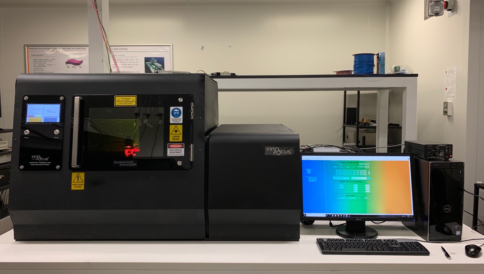
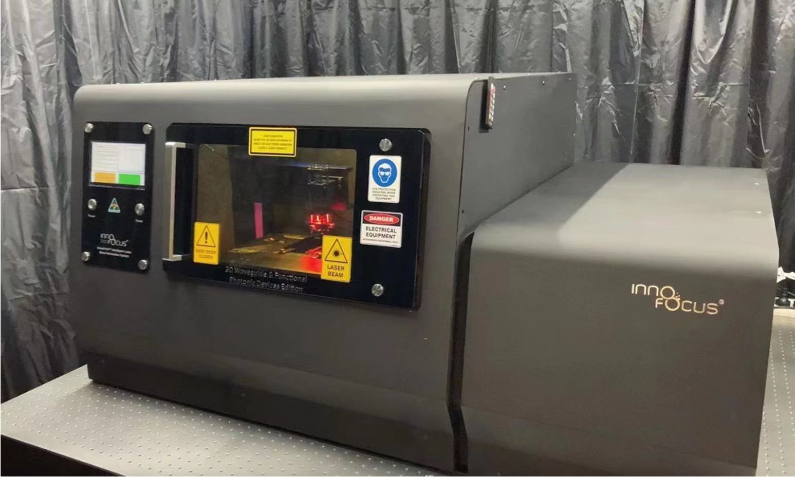
NanoPrint 3D Intelligent Laser Nano-fabrication System is one of Innofocus’ core product series, with world-leading technical capability and product performance.
Innofocus has a number of core technology invention patents in this domain, with complete intellectual property rights and independent manufacturing capabilities in the fields of optics, electromechanics, algorithms, and automated software systems.
Innofocus NanoPrint 3D Intelligent Laser Nanofabrication System meets the customers’ needs from both academia and industry.

We provide a full range of products, solutions, and services such as design and verification test services, sample fabrication services, system equipment product, customised product co-development, and standard application consumable devices.
Innofocus® has developed the NanoPrint system to automate the processing of micro and nano fabrication without the need for a tedious learning and training process, allowing for a quick start. A customised version is also available in addition to the standard system, allowing the system to be tailored to the specific needs of the researchers for their applications.
Femtosecond laser 3D nanofabrication technology, a high-performance laser direct writing technology with micro and nano processing scale, is more suitable for high-precision large-area complex structure in one go compared with traditional processing means. It has important significance and broad prospects in the research and application development fields of physics, chemistry, materials, electronics, mechanics, and biology, among other disciplines.
Our products provide intuitive interface, intelligent suggestions for parameter configuration, software packages based on different processing scenarios as well as standard operating procedures. Our production process pursues precision on each critical design detail, thus creating the best customer experience and improving the processing efficiency and results.
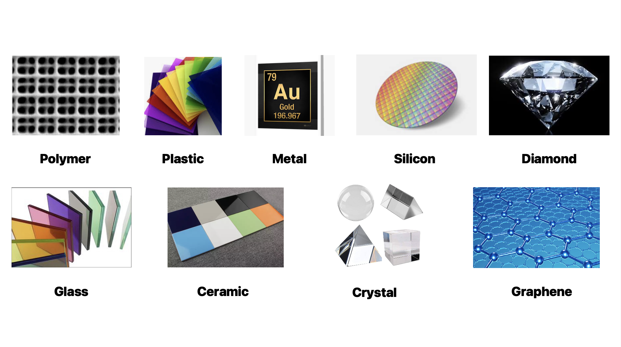
The laser of the Innofocus® system is selected to meet the highest performance specifications required for micro and nano laser fabrication: the wavelength, the tunable repetition rate, and the appropriate pulse width and high peak power. Depending on the field of research or application, the correct selection of these performance specifications will give the laser the greatest freedom in fabricating different materials. Depending on the requirements, the materials to be fabricated can cover a wide range of materials such as conventional polymers, glass, crystals, photoresists, metals, low-dimensional materials, solid dielectric materials, ceramics, etc. to achieve high precision fabrication.
The size and accuracy of the writing and positioning requirements vary according to the fabrication needs. Important indicators that affect the size and positioning accuracy include: range, maximum step length, positioning accuracy, maximum scanning speed, and maximum load capacity.
Innofocus offers users a wide range of system module options in terms of surface area and positioning accuracy to suit the technical needs and budget requirements of different research and industrial applications. In addition, our systems have the following advantages:
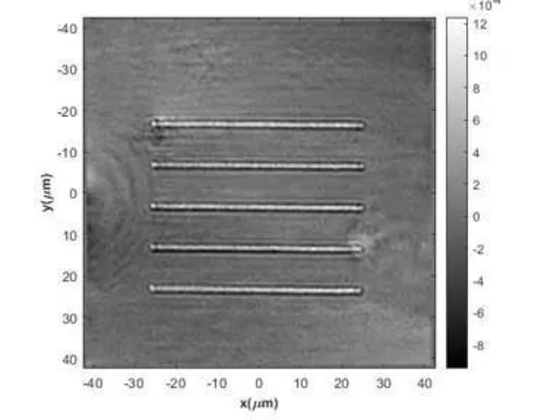
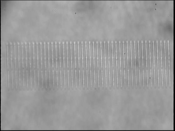
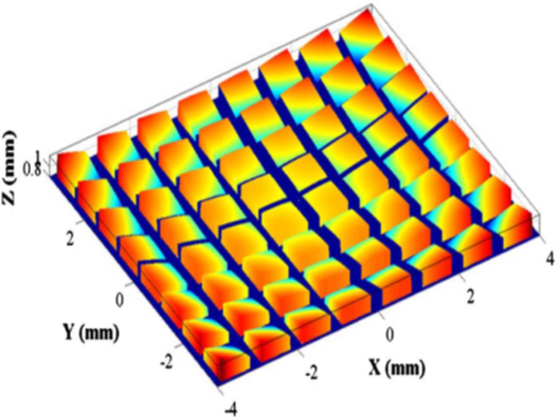
· The long range allows for the fabrication of large area optical components, offering the possibility of structure fabrication including optical waveguides, fiber gratings, WDMs and microlens arrays.
· Using the cutting-edge technology from Germany, this system solves the worldwide problems of extremely long range, extraordinarily small step lengths and high positioning accuracy, representing the highest level of scanning stage.
· High scanning speeds of 90 mm/s and even 2 m/s are achieved with nanometre-level accuracy, increasing the fabrication speed of structures and system productivity without loss of fabrication accuracy. Not only does it support large-area fabrication, but it also has a high load-bearing capacity, making it suitable for placing special fixtures for fabricating different materials and devices such as optical fibres, optical waveguides, and photonic wirebonding (PWB).
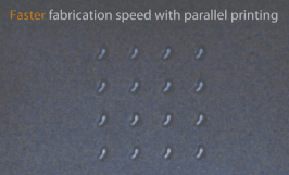
Conventional laser fabrication with a single focus is time-consuming and inefficient, but Innofocus®’s unique multi-focal fabrication technology increases fabricating speed and efficiency. The laser is processed in a periodic array structure in the crystal, and the focal intensity at each point can be controlled at will. By adjusting the spatial light modulator, the focal array and the intensity of exposure at each focus can be arbitrarily selected in a single exposure.
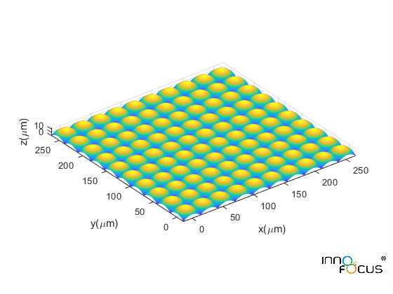
During waveguide fabrication, the fabricating position is relatively deep in the dielectric material due to its large dimensions. The aberrations caused by the accumulation of refractive index mismatches therefore have a significant negative impact on the fabrication. And this effect progressively worsens with increasing processing depth. Laser spot shaping therefore plays a pivotal role in the fabrication of micro-nano and waveguides.
Without aberration correction, the normal elliptical spot will be stretched with the peak spot energy being extremely dragged down, causing the fabrication to not proceed properly. After correction, the spot returns to normal and the process can be carried out normally as designed. As the machining depth increases, the unshaped spot completely overlaps and cannot form the structure that needs to be fabricated, while after shaping a high quality dot structure will be produced.
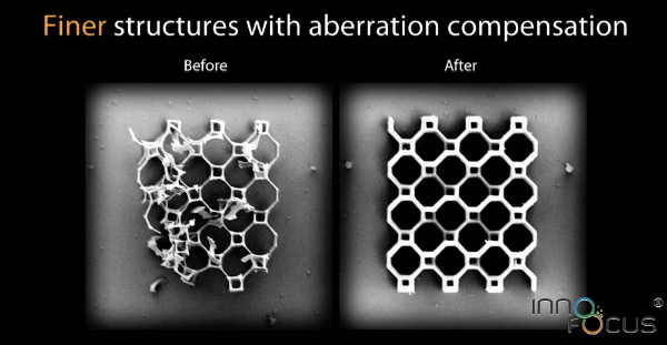
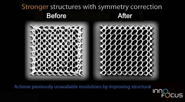
For waveguides, the ideal cross-sectional shape is circular. However, with conventional laser fabrication systems, due to the focusing characteristics of the microscope, the light spot is an ellipse along the z-direction in the x-z plane. This spot shape reduces the symmetry of the fabricated optical waveguide and ultimately increases the transmission loss of the optical waveguide.
The unique beam shaping method of the Innofocus® system enables a near-circular distribution of the laser focus in the x-z plane, thus significantly improved the fabrication quality and fidelity compared to the design structure.
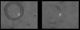
The imaging suite is an important characterization module in the laser direct writing system for achieving high spatial resolution imaging of the 3D refractive index distribution of the sample in real time and in situ during the laser direct writing process of optical waveguides and other optical devices, providing a quantitative basis for the optimization of laser power, repetition frequency and exposure time parameters in the laser direct writing process.
Innofocus implements in-situ characterization functions for optical devices such as optical waveguides in laser direct writing systems, enabling quantification and precision of the entire optical device preparation process. The resulting increase in preparation efficiency and the fabricating of devices more in line with theoretical design can achieve significant improvements in device performance and better serve scientific research and industrial applications for high-speed optical communications and precision optical sensing.
The refractive index imaging in-situ characterization module makes the laser direct writing system an invaluable key capability for optical device fabrication applications and describes Innofocus’ patented invention in four words: “quantitative, precise, intelligent and efficient”
Innofocus’ Nanoprint intelligent 3D laser nano-fabrication system has a number of patented inventions to achieve easier operation and better user experience:
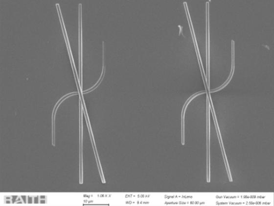
a) Suitable for the stringent requirements of a wide range of optical waveguide fabrication and for Photonic WireBonding (PWB) technology. The machine vision not only automatically finds the working surface, but also the position of the optical waveguide to which it is to be connected, enabling automatic machine alignment. The positioning accuracy of ±50 nm ensures smooth fabrication of the optical waveguides and avoids irreducible and high error rates in human alignment.
b) On this basis, the technique measures the tilt of the surface of the sample and changes the tilt of the surface of the optical waveguide to be fabricated accordingly, so that it remains parallel with the surface of the sample and thus achieves high coupling efficiency when used.
c) The surface of the two-dimensional material can be tracked in real time when working with large area two-dimensional materials, avoiding errors caused by surface tilting or distortion and improving the yield of the process. The surface of the three-dimensional material can also be tracked, enabling the fabrication of new devices.
d) The technology automatically finds the position of the fibre core and, through machine vision recognition, corrects the fabrication position in-situ, greatly improving the yield of the optical fibre grating processing. The technology can be applied to any material and pattern configuration of the fibre structure.
1. Any 2D and 3D structure can be imported and automatically converted into a file that is compatible with the system. Thus, the user can design the structure to be fabricated using any software, including 2D drawing and 3D design software. The direct conversion by the Innofocus®️ system software generates machining files quickly and efficiently;
2. The user can design the layer spacing and 3D resolution according to the required structure size to achieve optimum results;
3. The user can select different transformation modes, such as centreline, border, or face scan for different structures to achieve different fabrication methods and further increase efficiency;
4. The software automatically finds the optimum fabricating method by using the input system parameters such as line width, scanning method and laser power;
5. The generated fabrication files are displayed graphically in the software system. The visualisation of the structure helps the user to effectively determine whether the generated files meet the requirements, avoiding problems caused by improper design and greatly increasing the success rate of fabrication.
1. The user can observe the entire process in real time with a high-resolution in-situ viewing system;
2. By observing in-situ to determine whether the results of the process are sufficient to meet the needs;
3. The system can capture video in real time for further analysis of the process, optimization of experimental parameters and display of experimental results;
4. The video is also archived and can be used for exhibition or teaching purposes.
Innofocus' intelligent laser nanofabrication system also features multi-focal parallel fabrication technology, combining with the SOP-based visualized software, significantly increasing the processing speed and efficiency. The Innofocus®️ system has been designed with a user-friendly operating system with the following features:
1. The software process meets the SOPs required by the user, so that the user only needs to follow the prompts for each step to move on to the next step. The software system provides interactive prompts and minimises misuse. At the same time, it is easy to operate, quick to learn and requires no complex training;
2. The software has a parameter setting check function. If the user sets parameters that are not reasonable, the software gives a prompt and asks the user to confirm the parameters to ensure safe operation and maximum protection of the hardware;
3. The software provides fully automatic parameter setting, such as automatic laser power adjustment, speed, interval, fabrication position selection, etc.
1. Patented technologies such as surface autotracing technology, surface autolanding, and automatic fiber core tracing function, which are easy to use and enable safe and convenient fabrication process.
2. PTST fabrication control function, which enables the intelligent nanofabrication system to be triggered synchronously in both position and time, simplifying the user's operation, thus enhancing fabrication efficiency and improving user experience.
3. Innofocus's world's only in-situ refractive index characterization imaging function, which makes online inspection of laser fabrication outcomes and on-site correction of fabrication conditions possible.
4. A large LCD touch screen on the panel clearly displays the 3D structure of the target sample, provides real-time information on the progress of the fabrication and the time remaining, and allows the user to perform key operations with a single touch;
5. The system has a mobile phone APP to remotely view the processing progress status and alarm alert function, which can greatly liberate the freedom of the users and improve convenience and safety in the case of a long fabrication time.
Highly automated and truly intelligent laser nanofabrication system provides users with more options:
1. More applicable fabrication material choices, including but not limited to: polymers, glass, sapphire, optical fiber, etc.
2. More design formats, users can import fabricating files designed by any software, through Innofocus®️ built-in software to efficiently generate in-system files of fabrication
3. More application fields, including but not limited to: optical waveguide components, 3D microstructures, communication device design and processing, etc.
1. Aberration correction function, after correction, the spot returns to normal and the process can be carried out normally as designed.
2. Focal spot shaping function, The unique beam shaping method of the Innofocus® system enables a near-circular distribution of the laser focus in the x-z plane, thus significantly improved the fabrication quality and fidelity compared to the design structure.
3. 1024-step power control of precision, the icing on the cake, making the fabrication outcomes more accurate, reproducing your desired design outcome.
INNOFOCUS