

Product
Menu
Solution
Menu
Technology
Menu
For Scientific Research & Industry Modernisation.
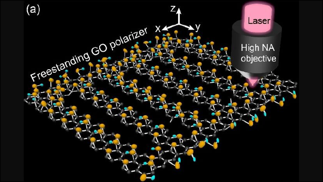
Fig. Freestanding GO polarizer
(Source from: Zheng, X., B. Xu, S. Li, H. Lin, L. Qiu, D. Li, and B. Jia, Free-standing graphene oxide mid-infrared polarizers. Nanoscale, 2020.
Mid-infrared (MIR) radiation, especially in the wavelength range from 3 μm to 30 μm, plays an indispensable role in a wide range of applications including infrared (IR) imaging and sensing, aerospace engineering, medicine, military defense, and information and communication. However, MIR-compatible (especially > 8 μm) materials are mainly limited to fragile, hazardous and expensive germanium selenide and fluoride-based materials such as Ge, ZnSe and BaF2, which remain challenging. It is critical to find suitable MIR materials with broadband MIR transparency, high refractive index, mechanical and chemical stability, cost effectiveness, and fast fabrication capabilities.
The discovery of graphene iso-excitations has attracted great interest due to the prospect of reshaping photonics and optoelectronics in MIR and terahertz (THz) modes. However, the poor processability and nanostructuring capabilities of graphene set limits to its practical MIR applications. In contrast, chemically derived graphene oxide (GO) is considered as an attractive alternative material due to the unique physical and chemical properties produced by hybridization. In particular, the optical and electrical properties of GO can be precisely tuned by the reduction process to enable various photonic and optoelectronic applications.
The current optical properties of GO have been limited in the visible or near-infrared (NIR) range by using conventional methods (e.g. ellipsoidal polarization, pictograms or microscopy). The optical properties of GO in the MIR domain have been rarely studied due to the limited choice of available MIR characterization methods and undisclosed material energy band models, which hinders its MIR photonic applications.
In the scheme, we prepared high-performance MIR polarizers with large extinction ratios (~20 dB) and controlled operating wavelengths in the MIR region by using laser nano-3D printing on a freestanding GO film.
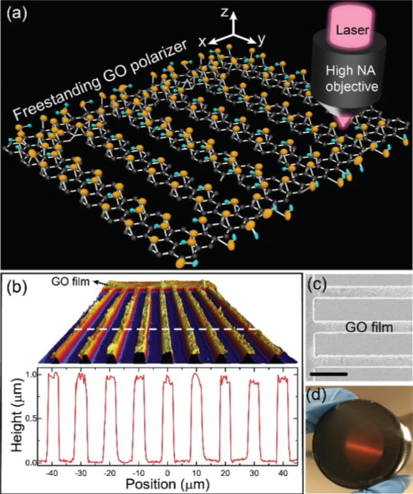
Fig. 1. Free-standing graphene oxide MIR polarizers (a) Conceptual design and laser manufacturing of the free-standing GO polarizer. (b) Top: The 3D topographic view of the GO polarizer measured with an optical profiler. Bottom: The cross-sectional surface profile of the GO polarizer along the white dashed line marked in the top 3D topographic view. (c) The SEM image of the fabricated GO polarizer. Scale bar: 10 μm. (d) The photo of a free-standing GO polarizer mounted on a commercially available standard polarizer mount.
Source from: Zheng, X., B. Xu, S. Li, H. Lin, L. Qiu, D. Li, and B. Jia, Free-standing graphene oxide mid-infrared polarizers. Nanoscale, 2020.
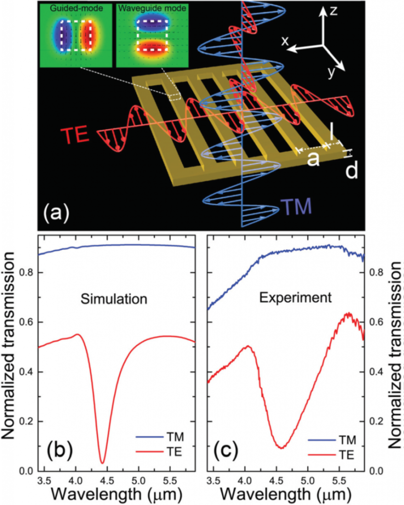
Fig. 2. The operations of graphene oxide MIR polarizers (a) Schematic figure of the working principle of the GO polarizer. Insets: The cross-sectional (x-z plane) electric field distributions within one exemplary GO rod (white dashed line) have been plotted for both guided-mode (left) and waveguide mode (right), respectively. (b) The FDTD simulation of the transmission spectra of the proposed GO polarizer under both TM and TE polarizations. (c) The experimental transmission spectra of the proposed GO polarizer measured by using the microscope FTIR spectrometer.
Source from: Zheng, X., B. Xu, S. Li, H. Lin, L. Qiu, D. Li, and B. Jia, Free-standing graphene oxide mid-infrared polarizers. Nanoscale, 2020.
The mechanical strength, low-cost manufacturing and flexible integration capabilities of freestanding GO polarizers offer great potential for a variety of photonic applications, especially in the MIR field
New optical components with atomic layer thickness can be realized in MIR or THz systems where materials are scarce.
INNOFOCUS

Can be used for infrared night vision, thermal imaging, multispectral imaging and infrared imaging.


Two-dimensional (2D) materials usually refer to materials containing single or multiple layers of atoms, ranging in thickness from single atomic layers to tens of nanometers. A variety of 2D materials such as graphene, boron nitride, transition metal sulfides, black phosphorus and chalcogenides have been successfully separated. Two-dimensional materials exhibit exceptional physicochemical properties, such as atomic layer thickness, strong nonlinear optical properties, magnetic properties, and excellent mechanical properties. These properties, which are very different from their block counterparts, create new opportunities for the application of 2D materials in nanodevices, especially in photonics.
Recently various 2D material micro/nanostructures and functional devices have been proposed and designed by various fabrication methods to achieve their excellent performance. Ultrafast laser direct writing technology has been widely used in material patterning, modification, and functionalization due to its rich mechanism and dynamics of light-matter interaction, special three-dimensional fabrication capability, flexibility of arbitrary structure design, and minimal thermal effects, which enable processing accuracy up to tens of nanometers and fully demonstrate its outstanding fabrication capability. Its ultra-high resolution and fabrication accuracy, simple and flexible fabrication methods and excellent cost performance are indispensable for the preparation of next-generation large-area, high-performance, portable, integrated and flexible devices.
The NanoPrint 3D Intelligent Laser Nano-fabrication System uses laser direct writing technology to prepare functional photonic devices such as ultra-thin lenses, graphene metamaterials, perfect absorbers, and holographic displays in 2D materials. In addition, ultrafast laser direct writing technology can be used for local nonlinear property modification of 2D materials by simply adding 2D material layers to conventional photonic devices and transforming them into highly nonlinear systems. This approach offers great flexibility to achieve ultra-fast speeds and greatly enhance the performance of all-optical communication systems.
In today’s society where everything is smart, sensors are playing an increasingly important role in our daily lives and in the Internet of Things. Sensors monitor our health (e.g. heartbeat), air quality, home security, and are widely used in the Industrial Internet of Things (IIoT) to monitor production processes. Our lives are surrounded by smartphones, wearables, and other smart devices, all of which are inseparable from sensors.
Widely used sensors in daily life include thermometers, pressure sensors, light sensors, accelerometers, gyroscopes, motion sensors, gas sensors and so on. Their design and manufacturing often rely on traditional electromechanical processing, which has a single function, large size and high energy consumption, and is not suitable for the new sensor miniaturization, integration, integration, high precision and low energy requirements. Therefore, how to innovate fabrication methods and improve the fabrication process has become a difficult problem in the field of sensing.
The NanoPrint 3D Intelligent Laser Nano-fabrication System can write flexible design and versatile 3D micro-nano structures in a variety of materials including polymers, 2D materials, metals, semiconductors, crystals, optical fibers, and other materials to form sensing mechanisms. Its writing method is flexible and simple to fabricate, and no vacuum or mask is required. More importantly, the written structure is small and highly integrated, and can form an immersion sensing with the substrate or environment. It is also possible to introduce in-situ high-precision sensors directly at the sites that need to be measured in sensing, without damaging the original environment and overall appearance.
In particular, graphene micro and nano sensors realized with NanoPrint system have been playing an important role in artificial skin, intelligent robots, health care, early diagnosis of diseases, wearable devices, etc. in recent years. In addition, FBG fabricated by the unique patented technology with NanoPrint system has the characteristics of easy operation, fast writing speed, stable process, flexible formation of a variety of special grating, and high raster rate. It solves the problems of expensiveness, complex process and single grating structure with the traditional fiber grating fabrication equipment. The formed FBG has large change in refractive index, high temperature resistance, high performance index and good stability, has replaced the traditional fiber grating and plays an irreplaceable role in the high temperature and high pressure environment.