

Product
Menu
Solution
Menu
Technology
Menu
For Scientific Research & Industry Modernisation.

Figure: Designed free-form optics (Source from: Design and fabrication of a freeform microlens array for a compact large-field-of-view compound-eye camera)
Free-form surface shapes lack translational or rotational symmetry about an axis perpendicular to the mean plane. Free-form optical devices include at least one free-form surface that lacks translational or rotational symmetry about an axis perpendicular to the mean plane, according to ISO standard 17450-1:2011. Non-imaging and illumination optics have utilized free-form surfaces since at least the 1990s.
The integration of free-form optics and surfaces into imaging systems remains a major challenge. However, the new degrees of freedom introduced by free-form optical design are the driving force behind overcoming these challenges. These additional degrees of freedom can lead to many potential advantages, including system miniaturization, reduced component count, and even bringing entirely new optical capabilities, all of which could have a profound impact on the optics industry. Manufacturing and metrology must go hand-in-hand with design to realize the full potential of free-form optics.
Traditional two-degree-of-freedom manufacturing processes such as grinding, polishing, and ultra-precision turning cannot produce free-form surfaces. In order to generate arbitrary free-form surfaces, higher degree of freedom processes such as axial diamond turning, diamond milling, and deterministic micro-grinding and polishing are required.
The additional degrees of freedom inherently increase the positioning uncertainty and make it difficult to simultaneously meet the optical designer's requirements for optical shape, mid-space frequency, and surface micro-roughness. Significant challenges remain in the metrology of free-form surfaces at this level because metrology stages normally have uncertainties comparable to those of manufacturing stages.
To address the problems of the above process, based on our understanding of fabricating micro-optical components, we recommend the method of using laser 3D nano-printing to fabricate free-form optical components. There are two possible methods:
1 polymer mask etching
This approach includes two main steps: 1) fabricating the structure of the microlens array in the polymer using laser nano-3D printing. 2) the microlens array of the polymer is then used as a mask and the pattern is transferred to the quartz substrate by etching.
2 Laser direct writing in quartz glass with selective acid etching
This method also includes two main steps: 1) using a high power laser inside quartz glass (which can be all kinds of glass) to write the antistructure of the microlens array to be fabricated (which is the structure to be removed by etching) directly through the phase transition introduced by the femtosecond laser 2) using selective acid etching to etch away the area to be removed.
Fig. 1. Designed free-form optics (Source from: Design and fabrication of a freeform microlens array for a compact large-field-of-view compound-eye camera)
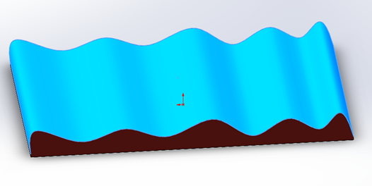
Fig. 2. Designing phase structure diagrams for free-form surfaces
Both of the above have a high degree of feasibility. However, the first method requires more requirements, including 1) the etching resistance of the photoresist, and 2) the cost of dry etching is relatively higher. Therefore, we recommend the second technique more. At the same time, although high-power femtosecond laser processing can directly etch the corresponding structure by laser ablation, the laser ablation method is based on the principle of micro-bursting, which may produce higher surface roughness. Therefore, we still recommend the introduction of material phase change on the surface of quartz glass by laser with selective etching to produce a surface that can achieve optical flatness and contribute to the improvement of imaging quality.
Based on laser 3D nano-printing technology, free-form optical components with arbitrary spatial distribution can be produced
The cost of laser processing is extremely low as no diamond turning is required, and the laser nanofabrication system developed by Innofocus allows for rapid design comparisons and thereby efficiently optimizing results.
The surface morphology of each component can be controlled independently. The high-resolution laser nano 3D printing technology enables the component's surface morphology to be fabricated in conjunction with each spatial location as needed.
Based on high accuracy and uniformity, accurate control of the quality of free-form optical components can be achieved, and high yield can be realized.
INNOFOCUS

Free form optical devices can be widely used in automotive lighting, optical imaging, radar ranging, infrared imaging


Micro-optical components are key components in the manufacture of small optoelectronic systems, which have the advantages of small size, light weight, low cost, and can achieve novel functions such as tiny, array, integration, imaging and wavefront conversion that are difficult to achieve with ordinary optical components. At present, miniaturization and integration of optical systems have become a major trend in various applications. Micro-optics are playing an increasing role in optical imaging and display systems, optoelectronic systems, laser devices, thermal imaging devices, night vision devices, infrared scanning devices, display systems, camera systems, zoom lenses, medical diagnostic fundoscopes, endoscopes, progressive lenses, cell phones, PDAs, CDs and DVDs, etc.
Driven by the application demand, the research on micro-optical component fabrication technology is also in progress. In addition to the traditional ultra-precision mechanical fabrication technology, a variety of modern fabrication technologies have also emerged, such as electron beam writing technology, photolithography, etching technology, replication technology and coating technology. These technologies are developed from microelectronic component microfabrication technology, but unlike the original electronic components, three-dimensional molding accuracy and assembly accuracy is critical for optical components, will directly affect their performance, so each of these methods has its own defects and limitations of use. Generally speaking, machining accuracy and machining speed and output are conflicting goals that are difficult to balance.
The fabrication of NanoPrint 3D Intelligent Laser Nano-fabrication system, based on the non-linear action of laser and matter, can realize three-dimensional high-precision micro-nano structures in a variety of materials, providing a new idea for micro-optical component fabrication. It also utilizes the technology of multi-focus parallel processing, which can increase the fabrication efficiency and productivity hundreds of times, pushing the laser direct writing technology from the laboratory to the production manufacturing environment.
The laser 3D nano-fabrication technology represented by NanoPrint system has realized the fabrication of aspheric lenses, microlens arrays, pyramidal microstructure surfaces, reflection-reducing gratings, free-form optical elements and other structures with advantages that traditional fabrication equipment does not have, such as flexible structure design, high precision and high speed. It is mainly characterized by the ability to fabricate true three-dimensional structures with nanometer-level precision.