

Product
Menu
Solution
Menu
Technology
Menu
For Scientific Research & Industry Modernisation.
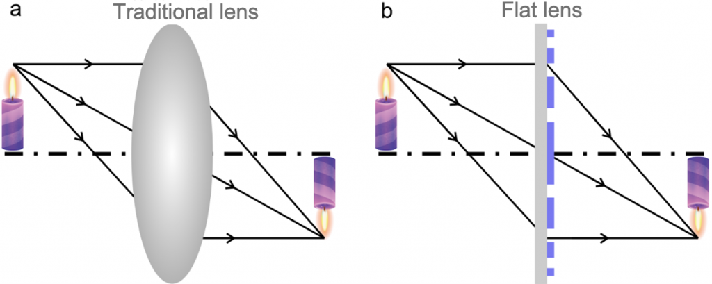
Lenses are one of the most common optical components used in everyday life. Whether it is the glasses that we normally wear, the lens that we use for taking pictures, the microscope that we use for research, or the magnifying glass that we use for the elderly, they are all lenses. The lenses used in daily life are spherical lenses, generally made of optical glass, optical crystals, optical resin and other optical materials. It uses the principle of optical refraction, using different materials, different spherical surfaces and different spatial positions to achieve control of light.
Conventional lenses are based on the principle of refraction, and the modulation of their wavefront is achieved by the optical range difference introduced by the thickness difference of the lens. The processing of conventional lenses requires processes such as material selection, cutting, rough grinding, fine grinding, polishing, and testing. Due to the limitation of its process, the surface morphology of the conventional lens can only be spherical, and the single lens cannot overcome the phase difference problem. At present, most cameras and microscope heads and other imaging systems stacks multi-layer lens to solve the problem of aberration. This leads to the current camera photography equipment is not only complex structure and very bulky.
Due to the above mentioned problems, scientists have been working to invent various methods to make lenses thinner. Fresnel lenses are an early method to make lenses thinner and are widely used in everyday life, such as flashing lights for cell phones. Fresnel lenses have a light surface on one side of the lens and concentric circles of varying diameters on the other side, from small to large. The use of aspheric, free-form surfaces can also reduce the overall optical length of a spherical mirror set and achieve the function of multiple lenses with one piece, improving the imaging quality while reducing the weight of the optical system. In addition, the use of diffractive elements to achieve the effect of a lens, such as diffraction gratings, computational holograms, and ultra-thin lenses developed on super-surfaces can also achieve effective modulation of light. Unlike conventional lenses, planar lenses achieve field and phase modulation of light by means of nanostructures on the surface. Therefore, by setting the nature of each nano-element and its spatial location, different functions such as achromatic, achromatic, controlling spatial resolution, achieving a special focused light field, and achieving super-resolution can be effectively integrated in a pure flat lens without the need for a complex lens set to accomplish this. Therefore, the use of ultra-thin pure flat lenses can significantly reduce the thickness and weight of current optical imaging systems and improve the imaging quality.
Based on the diffraction principle, the design of ultra-thin (thickness on the order of optical wavelength) flat lenses is possible through spatially ordered nanostructures. Ultra-thin flat lenses can significantly reduce the thickness of the optical device, with the use of very little material, reducing the mass of the system, and ultimately reducing the cost of the optical system. However, the thickness of currently available flat lenses for imaging is still on the order of optical wavelengths, and further reductions in the thickness of flat lenses are extremely challenging to achieve. If the thickness of the material is much smaller than the optical wavelength, high efficiency diffraction cannot be achieved, resulting in low resolution of the lens imaging, contrast degradation, etc.
The thickness of most planar lenses is still comparable to the wavelength, especially the equivalent wavelength within the material. From conventional lenses to planar ultra-thin lenses, there are still many engineering and optimization-oriented questions, such as the design of the introduction of adjustable mechanisms to improve prism focusing efficiency and broadband, color aberration aberration correction, and so on. But the most exciting scientific question is: how thin can the lens be? If the lens is a single atomic layer of two-dimensional material, is it still possible to make a lens? Currently, due to the limitations of the modulation principle, the need to achieve sufficiently strong field and phase modulation requires materials with sufficient thickness, in the order of optical wavelength, so that high-quality imaging can be achieved. Although some research works have been introduced to achieve focusing using lenses or mirrors with sub-nanometer thickness, their focusing efficiency is limited to less than 1%, which cannot meet the demand of high quality imaging. Often single atomic layer materials are considered too thin to provide sufficient phase or amplitude modulation to achieve the lens function, let alone a high efficiency focusing lens, and the classical design principles of diffractive lenses and superlenses are no longer applicable, so there are no available theoretical principles to guide, and even some sound contrary to common sense.

Fig. 1. Femtosecond laser fabrication of single atomic layer 2D materials for ultra-thin flat lenses (Source from: Lin, H., et al., Diffraction-limited imaging with monolayer 2D material-based ultrathin flat lenses. Light: Science & Applications, 2020. 9(1). )
This solution is based on the special interaction between the femtosecond laser and the monolayer 2D transition metal dihalide. When the femtosecond laser irradiates the surface of the monolayer 2D transition metal dihalide, its material decomposes and produces nanoparticles of transition metal oxides. Since the laser pulse of the femtosecond laser processing is very short, the material is not heated during the interaction and, therefore, is a cold process, and the resulting nanoparticles can be effectively adsorbed on the substrate surface to realize a pattern composed of nanoparticles.
The process is shown in Figure 1, with the focused femtosecond laser irradiating a single layer of transition metal dihalide material. The thickness of this monolayer is only 7Å, as shown in the inset in Figure 1. As seen in the enlarged view therein, nanoparticles of metal oxides were produced in the region irradiated by the laser. The produced nanoparticles have a strong scattering effect on light, which enables the modulation of the field intensity of light. Therefore, by arranging such nanoparticles into a structure of concentric rings by the femtosecond laser, a lens effect is achieved, enabling the focusing of light and the imaging of objects. The line width of each ring depends on the spatial resolution of the femtosecond laser focus. In this study, a high numerical aperture microscope head was used to focus the femtosecond laser to achieve high spatial resolution up to 400 nm.
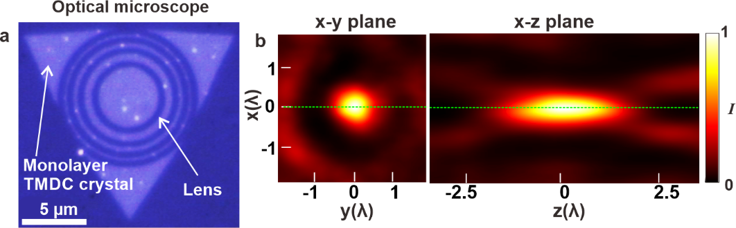
Fig. 2. Microscope picture of the fabricated single atomic layer lens and its focused light intensity distribution (Source from: Graphene Multilayer Photonic Metamaterials: Fundamentals and Applications)
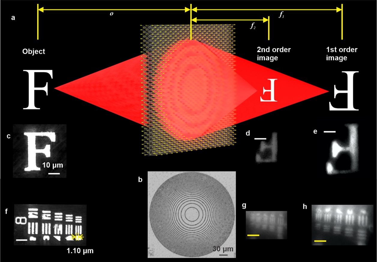
Fig. 3 Imaging of large-area atomic-level ultra-thin lenses (Source from: Lin, H., et al., Diffraction-limited imaging with monolayer 2D material-based ultrathin flat lenses. Light: Science & Applications, 2020. 9(1). )
An optical micrograph of a lens fabricated using laser fabrication is shown in Figure 2(a). The lens consists of concentric rings with unequal spacing. The area irradiated by the femtosecond laser is darkened due to the generation of nanoparticles that form a strong scattering of light. The light intensity distribution of its focused focus in the xy plane and xz plane is shown in Fig. 2(b), which achieves subwavelength resolution in the xy plane and wavelength-level resolution in the xz plane. The fabrication method can achieve good focusing effect in arbitrary single-layer transition metal dihalide materials. Its focusing efficiency can reach 31%, which is much larger than that of the current sub-nanometer-thick planar lenses.
Meanwhile, by fabricating a large-area monolayer transition metal dihalide lens, the first high-resolution imaging of a single atomic layer material lens was achieved in this study, and the results are shown in Figure 3. The letter F and a USAF standard plate were used to characterize the imaging effect. Two of the parallel lines at 1.1 μm can be clearly distinguished in the figure. More interestingly, since the lens can achieve both positive primary and positive secondary imaging, this allows for effective implementation of variable-focus lenses with different magnifications.
Based on femtosecond laser direct processing technology, 3D structures with arbitrary spatial distribution can be produced
Using femtosecond laser fabrication technology has a extremely low cost, and it also reduces the time consumed for design comparison thereby rapid optimization for processing.
Spatial refractive index distribution of optical waveguides can be precisely controlled due to the high-quality laser nanofabrication technology.
INNOFOCUS

By integrating this lens into cameras, VR/AR devices and microfluidic devices, we can effectively reduce the size and thickness of the devices and achieve the special functions required by customers. It can be widely used in micro-spectrometer, ultra-thin digital camera, microfluidic device, optical communication device, phase modulation device, transparent phase plate, holographic optical element, VR/AR device.


Two-dimensional (2D) materials usually refer to materials containing single or multiple layers of atoms, ranging in thickness from single atomic layers to tens of nanometers. A variety of 2D materials such as graphene, boron nitride, transition metal sulfides, black phosphorus and chalcogenides have been successfully separated. Two-dimensional materials exhibit exceptional physicochemical properties, such as atomic layer thickness, strong nonlinear optical properties, magnetic properties, and excellent mechanical properties. These properties, which are very different from their block counterparts, create new opportunities for the application of 2D materials in nanodevices, especially in photonics.
Recently various 2D material micro/nanostructures and functional devices have been proposed and designed by various fabrication methods to achieve their excellent performance. Ultrafast laser direct writing technology has been widely used in material patterning, modification, and functionalization due to its rich mechanism and dynamics of light-matter interaction, special three-dimensional fabrication capability, flexibility of arbitrary structure design, and minimal thermal effects, which enable processing accuracy up to tens of nanometers and fully demonstrate its outstanding fabrication capability. Its ultra-high resolution and fabrication accuracy, simple and flexible fabrication methods and excellent cost performance are indispensable for the preparation of next-generation large-area, high-performance, portable, integrated and flexible devices.
The NanoPrint 3D Intelligent Laser Nano-fabrication System uses laser direct writing technology to prepare functional photonic devices such as ultra-thin lenses, graphene metamaterials, perfect absorbers, and holographic displays in 2D materials. In addition, ultrafast laser direct writing technology can be used for local nonlinear property modification of 2D materials by simply adding 2D material layers to conventional photonic devices and transforming them into highly nonlinear systems. This approach offers great flexibility to achieve ultra-fast speeds and greatly enhance the performance of all-optical communication systems.
Micro-optical components are key components in the manufacture of small optoelectronic systems, which have the advantages of small size, light weight, low cost, and can achieve novel functions such as tiny, array, integration, imaging and wavefront conversion that are difficult to achieve with ordinary optical components. At present, miniaturization and integration of optical systems have become a major trend in various applications. Micro-optics are playing an increasing role in optical imaging and display systems, optoelectronic systems, laser devices, thermal imaging devices, night vision devices, infrared scanning devices, display systems, camera systems, zoom lenses, medical diagnostic fundoscopes, endoscopes, progressive lenses, cell phones, PDAs, CDs and DVDs, etc.
Driven by the application demand, the research on micro-optical component fabrication technology is also in progress. In addition to the traditional ultra-precision mechanical fabrication technology, a variety of modern fabrication technologies have also emerged, such as electron beam writing technology, photolithography, etching technology, replication technology and coating technology. These technologies are developed from microelectronic component microfabrication technology, but unlike the original electronic components, three-dimensional molding accuracy and assembly accuracy is critical for optical components, will directly affect their performance, so each of these methods has its own defects and limitations of use. Generally speaking, machining accuracy and machining speed and output are conflicting goals that are difficult to balance.
The fabrication of NanoPrint 3D Intelligent Laser Nano-fabrication system, based on the non-linear action of laser and matter, can realize three-dimensional high-precision micro-nano structures in a variety of materials, providing a new idea for micro-optical component fabrication. It also utilizes the technology of multi-focus parallel processing, which can increase the fabrication efficiency and productivity hundreds of times, pushing the laser direct writing technology from the laboratory to the production manufacturing environment.
The laser 3D nano-fabrication technology represented by NanoPrint system has realized the fabrication of aspheric lenses, microlens arrays, pyramidal microstructure surfaces, reflection-reducing gratings, free-form optical elements and other structures with advantages that traditional fabrication equipment does not have, such as flexible structure design, high precision and high speed. It is mainly characterized by the ability to fabricate true three-dimensional structures with nanometer-level precision.